Maskless Laser Direct Imaging Lithography Tool Creates NanometerPrecise Designs The DailyMoss
We are an innovative supplier of laser direct imaging (LDI) system solutions for various PCB manufacturing environments and adjacent markets. Our system product portfolio ranges from LDI system configurations for high-mix and emerging PCB niche applications up to fully automated LDI system solutions for mass production environments.
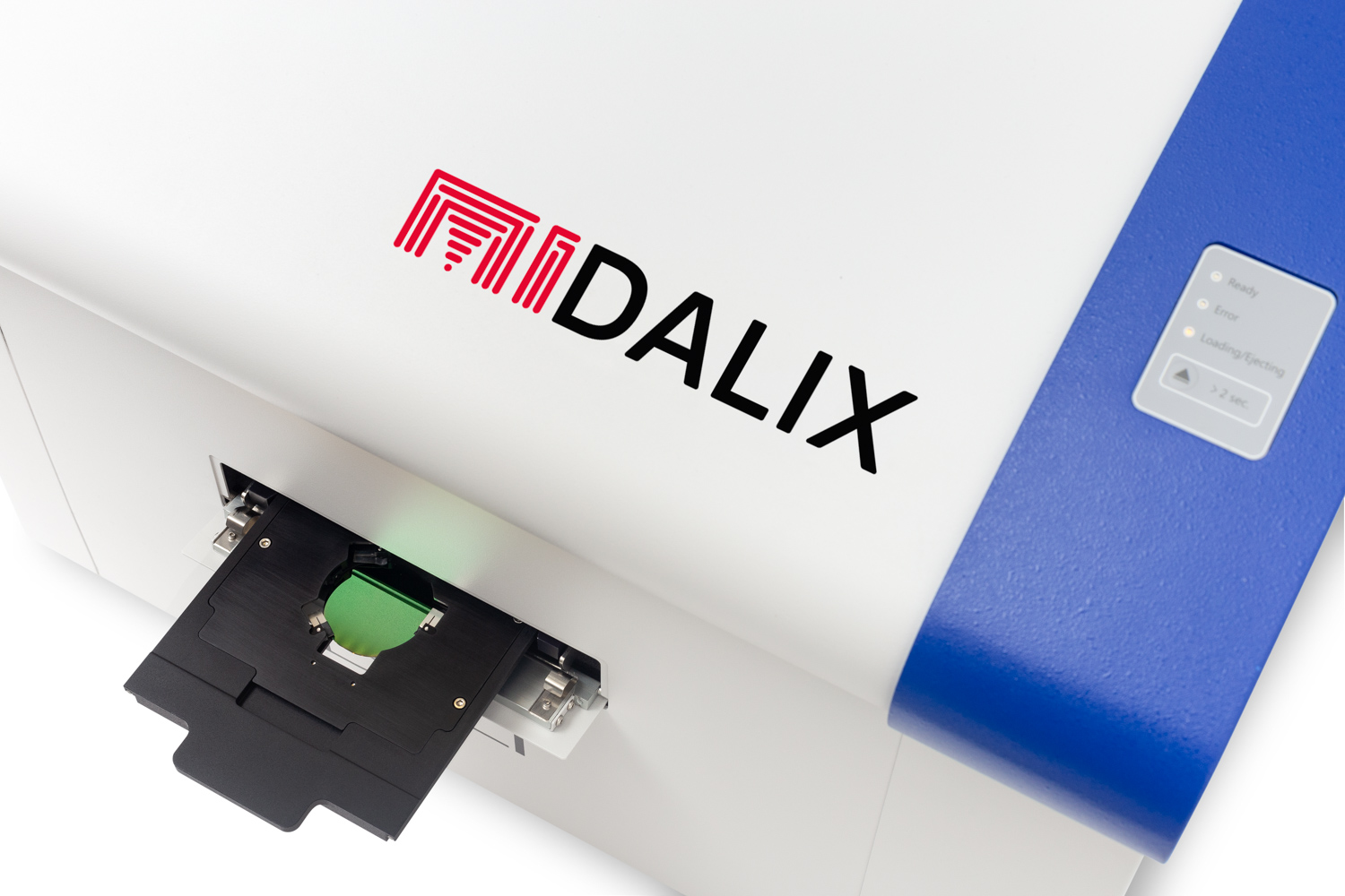
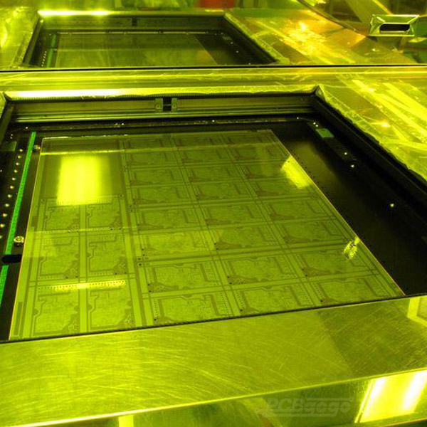
PCB Laser Direct Imaging LDI Equipment 610x710mm
We are an innovative supplier of Laser Direct Imaging (LDI) system solutions for various PCB manufacturing environments and adjacent markets. Our system product portfolio ranges from LDI system configurations for high-mix and emerging PCB niche applications up to fully automated LDI system solutions for mass production environments.

LED Laser Direct Imaging system PNC Inc.
process. Continuing to derail the cost drivers associated with laser direct imaging will further enable LDI processing to play a leading role in PWB manufacturing today and into the future. Laser direct imaging for printed wiring board (PWB) applications emerged in the mid 1980's. The LDI systems offered at that time suffered from a variety of
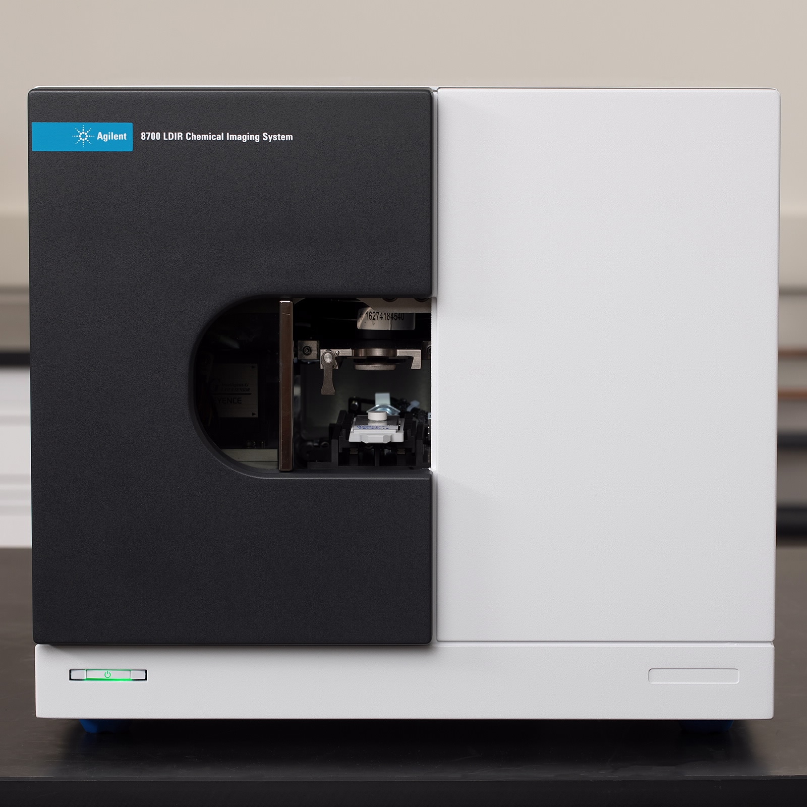
Agilent 8700 LDIR Laser Direct Infrared Imaging SRA Instruments
LDI provides a number of advantages: Quality - photo film issues in the past have resulted in imperfect images due to inherent susceptibility to fluctuations in temperature or humidity. Laser images result in much more precise and consistent images, and eliminate any film-related defects. Laser imaging provides precise positioning and.
Explaining Laser Direct Imaging in PCB Fabrication by PCBGOGO
Laser Direct Imaging (LDI) is a cornerstone of high precision PCB fabrication. Adoption is on-going so it costs more than traditional fabrication. Nobody wants to overspend on their Printed Circuit Board. One way to overspend is to find yourself scrapping boards because their construction didn't meet the stated performance objectives.
Laser Direct Imaging (LDI) PCB PLI International
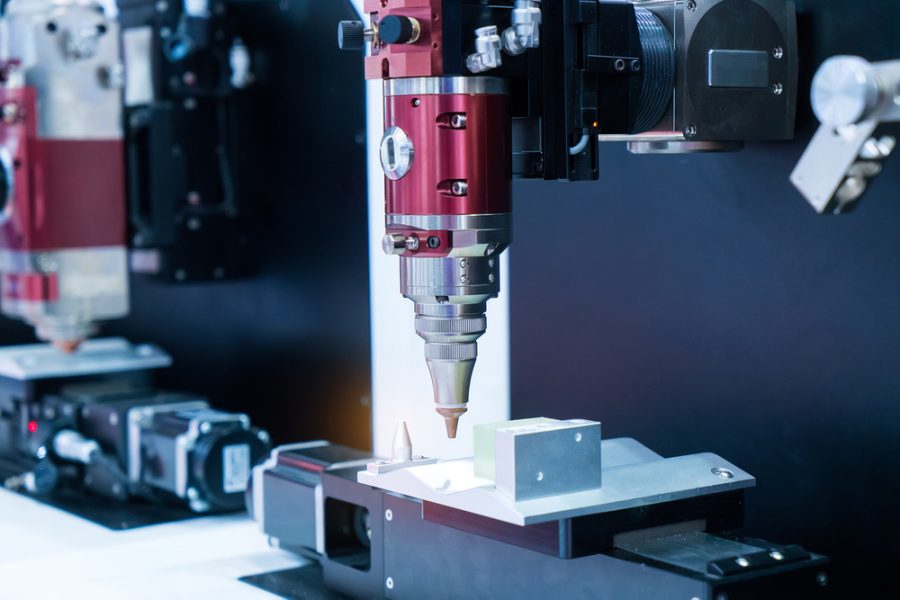
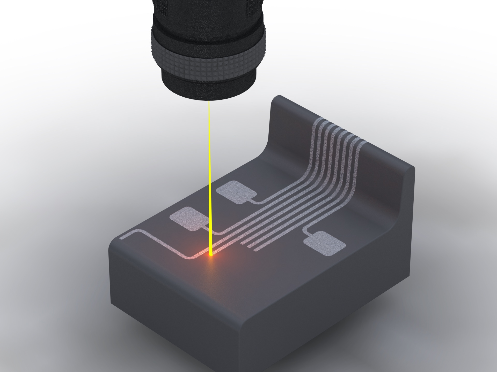
Laser Direct Imaging is the next step in the evolution of the PCB photolithography process. Unlike photo exposure, LDI does not employ a phototool. It directly exposes a digitally saved pattern onto the resist. Photoresist is selectively exposed to the laser beam in increments across the substrate in a rastering manner.

Agilent 8700 Laser Direct Infrared (LDIR) Chemical Imaging System Video YouTube
KLA Announces Second Quarter Fiscal Year 2024 Earnings Date. November 15, 2023. KLA Announces Upcoming Investor Webcasts. November 2, 2023. KLA Declares Regular Cash Dividend. News. KLA is a leader in process control using advanced inspection tools, metrology systems, and computational analytics. Keep Looking Ahead.
Laser Direct Imaging LDI in PCB Manufacturing
Designed for advanced high-density interconnect (HDI) including modified semi-additive processes (mSAP) and IC substrate mass production, this integrated system enables super-fine, highly uniform lines with outstanding accuracy, creating new opportunities for manufacturers and designers.
Explaining Laser Direct Imaging in PCB Fabrication by PCBGOGO
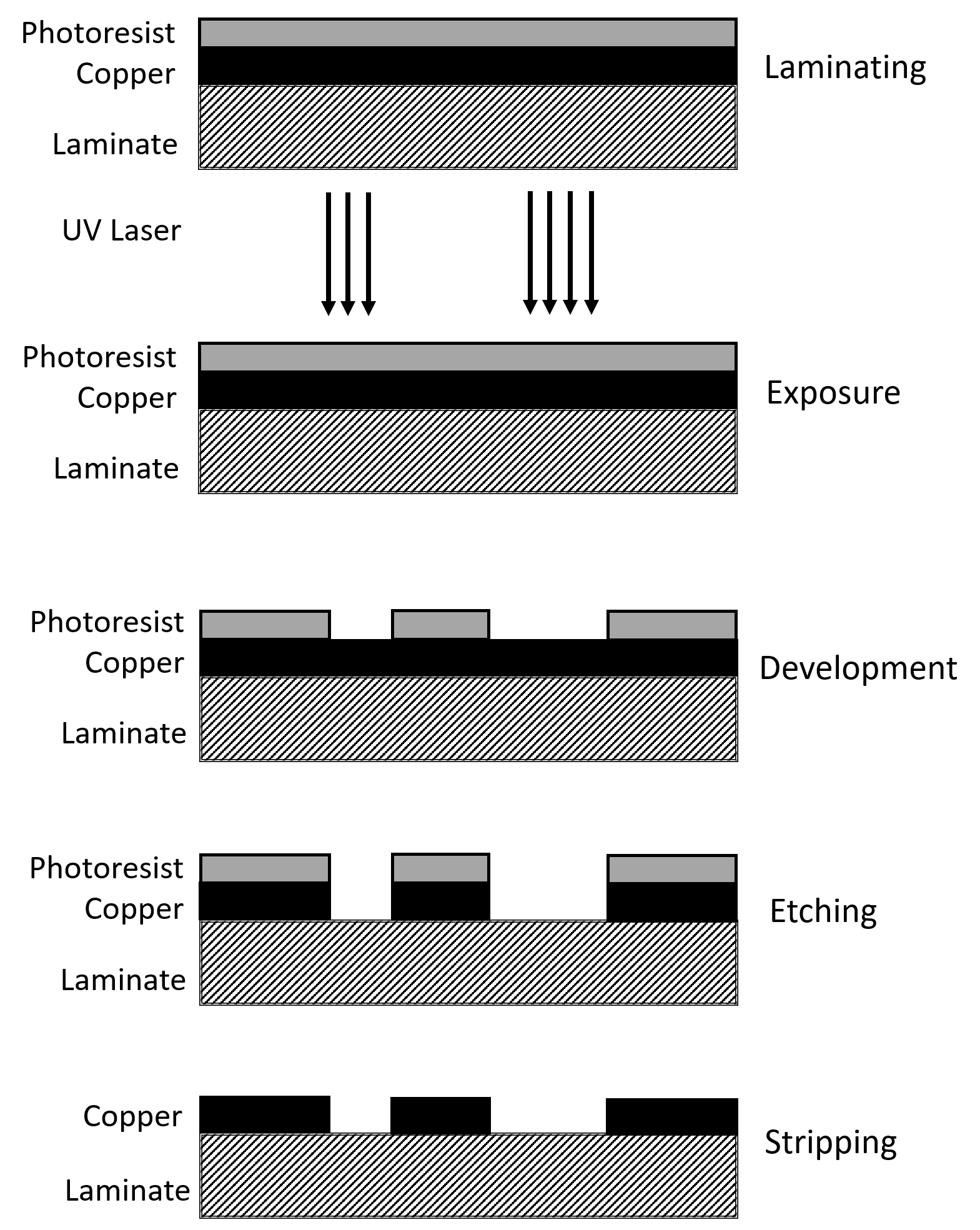
PRODUCT FEATURES/ APPLICATIONS Negative working, aqueous processable dry film photoresist with very high photospeed. Especially developed for exposure using UV laser direct imaging. Available in 30 micron (1.2 mil), and 50 micron (2.0 mil) thicknesses. Suitable for print and etch application with acid or alkaline etching.

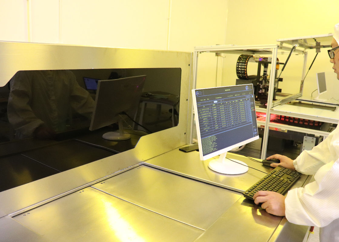
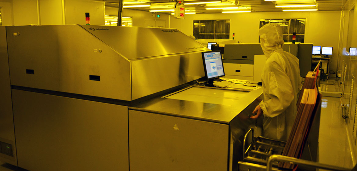
Laser Direct Imaging system accurately images PCB panels
Laser Direct Imaging (LDI) in the production of printed circuit boards (PCBs) offers a number of advantages over traditional contact printing methods. This paper reviews the basics of LDI technology and explores how solid state laser technology has positively impacted system throughput and cost-of-ownership characteristics. 1 LDI Basics In LDI, a laser is used to image a pattern directly on to.
PCB Fabrication With Laser Direct Imaging
Laser direct imaging (LDI) is a technique that uses high-intensity ultraviolet light to initiate a chemical reaction within a resist. As a result, the resist hardens. This imaging method can be applied to prototype circuit boards with wide trace widths.

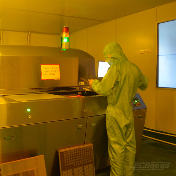
Making PCBs with laser direct imaging YouTube
LDI, or Laser Direct Imaging, is a technology used in Printed Circuit Board manufacturing emerged as a response to the increasing complexity and miniaturization of electronic devices. As PCBs become more densely packed with finer features, traditional photolithography methods using photomasks have limitations in meeting these advanced requirements.
Electronic assemblies without PCBs but with Laser direct structuring
In response to new electronics tendencies, the PCB manufacturing industry has come up with a new imaging technique known as Laser Direct Imaging. Below you will find an introductory guide to this process. What exactly is LDI? When a circuit board is made, the imaging process is what defines the circuit traces.
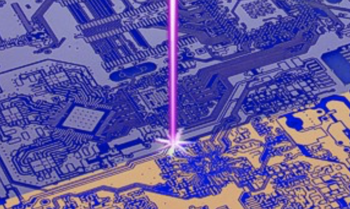
The scheme of the Laser Direct Imaging (LDI) process [1]. Download Scientific Diagram
Laser Direct Imaging is the evolution of the PCB photolithography process. LDI does not adopt photo tool, but directly exposes the patterns of Gerber file onto the photoresist film. This UV photoresist is selectively exposed to the UV laser beam in increments across the laminate in a raster manner.
Laser Direct Imaging and its advantages Sierra Circuits
Agilent 8700 Laser Direct Infrared (LDIR) Chemical Imaging System Video. In this video demonstration see how the 8700 LDIR uses the latest Quantum Cascade Laser (QCL) technology coupled with rapidly scanning optics to provide fast, clear, high-quality images and spectral data.

(PDF) Laser Direct Imaging of the Printed Electrical Circuits on PCB
The use of laser direct imaging (LDI) processing for outer layer circuit pattern generation and the benefits already obtained with this process have encouraged attention to be focussed on the possibility of using laser direct imaging soldermask (LDISM) in the secondary imaging stage of printed circuit board (PCB) fabrication.